
Apple A4 Teardown
Duration: 45 minutes
Steps: 33 Steps
Taking apart processors like the A4 is usually a top-secret mission handled by a select few global tech detectives. These reverse engineering teams are like the Sherlock Holmes of electronics, tracing who made which circuits and what clever tricks they used to build them. They dig into processors, audio controllers, and every single piece inside your cellphone or tablet, uncovering layer by layer how each chip is put together. We've teamed up with the semiconductor sleuths at Chipworks to give you a behind-the-scenes look at how these chip teardowns happen, as well as an exclusive peek inside the iPad’s hardware. The Chipworks crew is just as curious about electronics as we are. Their deep dive into the iPad’s chips will help you understand what makes your tablet tick—practically at the atomic level.
Step 1


- Meet the A4 microprocessor: the powerhouse behind the iPad.
- On the A4 chip, you'll spot the silkscreen label N26CGM0T APL0398 339S0084 YNL215X0. It looks like a secret code, but honestly, it’s not something we need to stress over. Let’s dive in and see what’s really going on inside.
- The A4 is an ARM-based processor that uses package-on-package design, which helps speed up and streamline the device’s internal workings.
Step 2

- When the original iPhone launched, we teamed up to take apart the processor. Our gear wasn’t as high-tech as what Chipworks uses today, but it got the job done just fine.
- Here’s a silicon wafer. Each tiny square you see is a chip, or a die. The A4’s processor die measures 7.3 mm on each side, totaling 53 square mm. The percentage of usable dies you get from a wafer like this is called the yield.
- The A4 isn’t just a processor—it’s a Package on Package (PoP). Actually, it contains three silicon dies stacked inside!
Step 3

- Getting ready to step into the cleanroom for some serious silicon action on the original iPhone—let's gear up and make this repair smooth and safe!
Step 4


- First things first: let's get that processor off the main board before we dive into the guts of it all.
- When it comes to unseating a processor from its cozy circuit board home, you've got two options: sheer brute strength or a little heat magic. Can you guess which method we went with?
Step 5


- Alright, let's get a little adventurous! First, we're going to slice that processor right down the middle for a fantastic cross-section snapshot. It's like a selfie for your tech!
- Now, hold on – we won't be using any heavy-duty band saws here. Instead, we'll take it nice and easy, carefully grinding through the processor and taking off tiny bits of material as we go. Slow and steady wins the race!
- And just a heads up, capturing a crystal-clear photo of a package's cross-section can be a bit tricky. The processor is one of the bigger packages in the iPhone, but it can be a bit sensitive. Just think about trying to do this with something half its size – it's a real challenge!
Step 6

- So, what exactly is a package? Well, take a look at this beauty right here!
- This image shows a cross-section of the iPhone's ARM processor combined with its RAM package. Click here to admire it in all its stunning 2854x313 resolution.
- In the center, you'll find the processor, which is the main rectangle. Below it, the shiny silver circles are the solder balls, doing their job to keep everything connected.
- Above the processor, there are two rectangles representing the RAM dies. They’re cleverly offset to create space for the wirebonds, which are a bit shy and aren't visible in this shot.
- Having the RAM so close to the processor is a clever move—it speeds up RAM access and cuts down on power consumption, which means your battery can last longer. How cool is that?
Step 7


- Welcome to the workbench! We love Weller for soldering, but any trusty tools will do the trick.
- Here are some tools that would have MacGyver grinning… although, he'd probably use a paperclip and some duct tape to get inside the processor. Let's get started!
Step 8

- Welcome to the world of cleanrooms—where everyday folks, just like you, gear up and enter spaces like this to work their magic. It's crucial to keep those pesky dust bunnies, lint, and hair at bay while you tackle your task.
- Tools of the trade:
- Scanning electron microscopes
- High resolution X-ray machines
- Really big magnifying glasses and microscopes
- And a bunch of other cool gadgets you might find in Q's lab
Step 9

- If only all safety issues were this quick and simple to fix!
Step 10

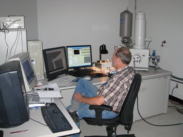
- Chipworks is located in Ottawa, Ontario, where the winters are so chilly that tires can actually crack if you're not careful! So, make sure to keep an eye on your wheels.
- The equipment at Chipworks is pretty unique compared to what you'll see in most semiconductor facilities. Each machine is designed with a single mission: to uncover the secrets hidden inside the latest chips. It's like a treasure hunt, but for tech!
Step 11

- Time for a close-up! We're diving into microscope analysis—think optical and SEM microscopes, not your average classroom gear.
- Precision is the name of the game here, and Salvation Repair is dialed in for accuracy. Every detail counts!
Step 12

- Check out the scanning electron microscope (SEM) doing its thing! This powerful tool lets you zoom in on tiny details—way beyond what an optical microscope can show. Just another cool gadget in the Salvation Repair toolkit.
Step 13

- Time to get grinding! As you work on leveling down that package, keep an eye on making sure everything stays nice and even. It’s super important!
- This part can feel like a marathon, but trust us, there's a true skill to grinding down to just the right spot while keeping a flawless surface. Think of it as a craft!
- We admit, we're not the best at this part, but that’s why we sometimes send our iPads to the pros at Chipworks!
Step 14


- First up, let's get rid of that outer packaging. It's gotta go!
- Time for a little science magic! We're diving into an acid bath.
- By submerging the processor in acid, we can melt away the ceramic casing that protects the silicon inside. Remember, using the right acid concentration for the specific ceramic is super important!
- Every now and then, taking a peek at a die can reveal some cool surprises hidden by the manufacturers. Unfortunately, we didn't find Milhouse in the iPad, but he did pop up recently in a Silicon Image chip!
Step 15


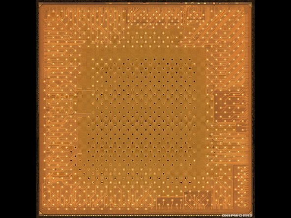
- Alright, now you’ve got the basics down. But what does the A4 look like inside?
- Check out these shots of the top and bottom of the A4 chip.
- Those tiny dots you see underneath are solder balls that secure the processor to the logic board. They handle all the power, grounding, and data transfers between the processor and the board.
Step 16

- Before we crack it open, let's take a peek inside with an X-ray to see what’s going on under the hood of that A4 processor.
- Zoom in and you’ll spot a bunch of tiny wirebonds looking like little threads—these are the pathways sending signals between different layers.
- The A4 chip is stacked in three layers: two layers are RAM (Samsung K4X1G323PE) and the third is the actual microprocessor.
- This clever Package-on-Package design means Apple can pick RAM from any supplier they fancy—they’re not stuck with just Samsung!
Step 17


- Check out these two side X-rays of the A4 processor.
- They’re snapped at two different focus points across the processor’s width. Took them quickly, so if they’re a bit fuzzy, that’s just part of the charm.
- The A4’s DRAM is Samsung-made, which means the wirebonds come from both sides—pretty unique compared to other DRAM modules we’ve seen.
- Those dark dots inside the processor? They’re solder balls linking the dies together. In the biz, those are called Ball Grid Arrays (BGAs).
Step 18

- Here we have an 8-layer die made of metal—pretty fancy stuff!
- Every iPhone processor we've peeked at had a Samsung part number stamped right onto the processor die. But guess what? We didn't spot any Samsung markings on the A4 (except for the DRAM). That's a solid clue that Apple is steering the semiconductor ship.
- We don't expect to see PA Semi (aka Apple's latest tech whiz acquisition) logos around here, but it's a safe bet they've played a key role in putting this chip together.
Step 19

- Here’s the SDRAM inside the A4 chip. Yep, that’s the Samsung logo—but no, Samsung didn’t design the A4, they just made the RAM.
- You’re looking at Samsung’s 1 Gb mobile DDR SDRAM (two of them).
- Each memory chip has the part number K4X1G323PE stamped on it.
- Breaking down that part number reveals there’s 2Gb of memory total, which means about 128MB per chip, adding up to 256 MB altogether.
Step 20


- Now that we've peeked inside, what are our takeaways?
- That's a wrap on the A4! Let's dive into some of the other chips hanging out inside the iPad.
- Nothing groundbreaking here. In fact, the A4 is quite reminiscent of the Samsung processor in the iPhone.
- From both the hardware and software, it’s clear this is a single-core processor, so it's definitely the ARM Cortex A8, not the rumored multicore A9.
- Identifying block-level logic inside a processor can be a bit tricky, so to pinpoint the GPU, we’re turning to software: early benchmarks suggest it's got similar 3D performance to the iPhone, leading us to believe the iPad is using the same PowerVR SGX 535 GPU.
- The iPad comes equipped with 256 MB of RAM, just like the iPhone.
- The A4 is a power sipper. In fact, its low power consumption likely explains why Apple hasn't cranked up the performance much from the iPhone. To achieve that impressive 10 hours of battery life, the whole iPad (display included) has to keep its average draw below 2.5 Watts.
Step 21

- Let's get into the nitty-gritty of your capacitive touchscreen controller, shall we? We're talking about the Broadcom BCM5974 here, a real champ in the touchscreen world. With a little patience and some handy tools, you’ll have your device back in action in no time. Just take it step by step, and remember, if things get too tricky, you can always schedule a repair with us. You've got this!
Step 22

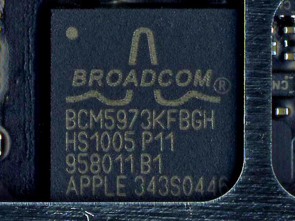
- Time to get hands-on with your device! First up, let's talk about the I/O microcontroller from Broadcom (it's the one that makes the touchscreen tick). You'll want the Broadcom BCM5973KFBGH HS0951P11 952280 B1 for the job. This little guy does all the touchscreen magic, so handle with care!
- Next, you're going to need the Apple 343S0446 chip. It's an essential part of your device's functionality, so make sure you’ve got the right one lined up. It'll keep everything running smoothly once you’ve got it in place.
Step 23


- Meet the Texas Instruments touchscreen line driver, the unsung hero behind your touchscreen magic.
- CD3240A 01D5AKT G1 – sounds like a secret code, but trust us, it's all about that smooth touchscreen experience!
Step 24
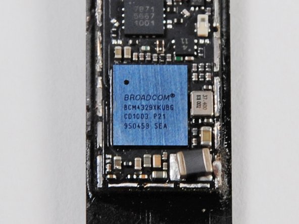

- Time to meet the magic behind your wireless connections! Here’s the Broadcom 802.11a/b/g/n WiFi plus Bluetooth 2.1 + EDR and FM combo. It’s like the social butterfly of your device, keeping all your signals flying.
- Spot the Broadcom BCM4329XKUBG CD1004 P21 chip, the little genius that keeps you streaming, chatting, and grooving. Give it a nod—it’s working hard to keep you connected!
Step 25


- Check out the Cirrus Logic device – it's likely the audio processor causing the issue.
- Look for the Apple 338S0589 B0 YFSAB0PY1001 part number to verify the component.
Step 26
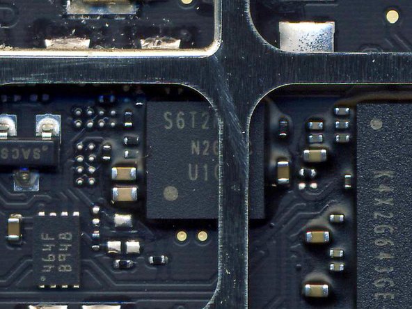

- It seems like we've got a little power management mystery on our hands. Let's dive into the details with model numbers S6T2MLC, N2266XQT, and U1003 A1. Remember, tackling these issues can be tricky, but you're doing great! If you find yourself in a bind, don't hesitate to schedule a repair for a helping hand.
Step 27

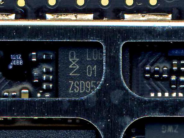
- Time to wrangle the mux/demux component for those DisplayPort and PCIe signals! Get hands-on with the NXP L0614 01 37 ZSD950 chip and make those connections behave.
- If this step feels like a brain-buster, you can always schedule a repair.
Step 28

- Screen time! Let's take a look at the LG SW0627B 01SWL-0032C 1003 N23977ON display. Handle carefully, and keep those fingerprints off for a crystal-clear finish.
Step 29


- Meet the Apple 338S0805 A2 e1 10028HBB chip! Ready to swap it out? Let’s roll up our sleeves and get this micro adventure started.
Step 30

- Accelerometer (identified by the ASIC and MEMS device die markings) - STM-LIS331DLH.
- STMicroelectronics 2949 33DH OK2 CL
Step 31

- DC-DC regulator.
- Linear Technologies 3442 N7667 LT9L
Step 32

- Intersil i976 45AIRZ F95OHX
Step 33

- That's our progress so far—stay tuned for more photos as they roll in!
- Big shoutout to the folks behind the scenes for their awesome work.
- If you're curious about a full breakdown, check out our iPad Teardown for every detail.


