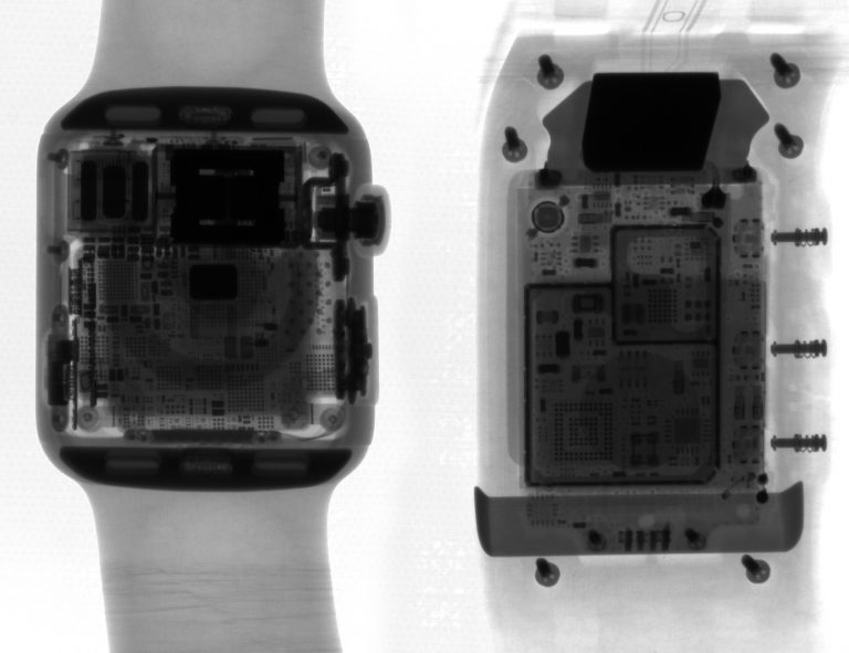
Apple Watch X-ray Teardown
Duration: 45 minutes
Steps: 20 Steps
The Apple Watch is quite the fascinating gadget! We gave you a peek inside it during our Apple Watch teardown, but now we're diving deeper. Thanks to our pals at Creative Electron, we're blasting this little marvel with X-rays to reveal its hidden secrets! Join us on this exciting journey into the unseen—it's time for a density teardown! Want to keep up with the latest device explorations? Slip on your X-ray specs and follow us on Instagram, Twitter, and Facebook! And remember, if things get tricky, you can always schedule a repair.
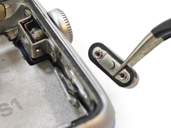
Step 1


We got into the zone. And before we knew it, they became our new best buddies.
- Once upon a time, Creative Electron shared an eye-popping X-ray teardown of the iPhone 6. Recently, some sharp-eyed tech enthusiasts got to spend a day exploring the magic of science firsthand at their labs in sunny San Marcos, CA. Creative Electron’s lineup features: a series of super-cool X-ray inspection systems, a talented crew of employees, and some seriously insightful features. If you need a hand with your repairs, you can always schedule a repair to get expert help.
Step 2


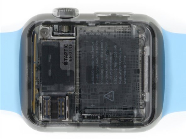
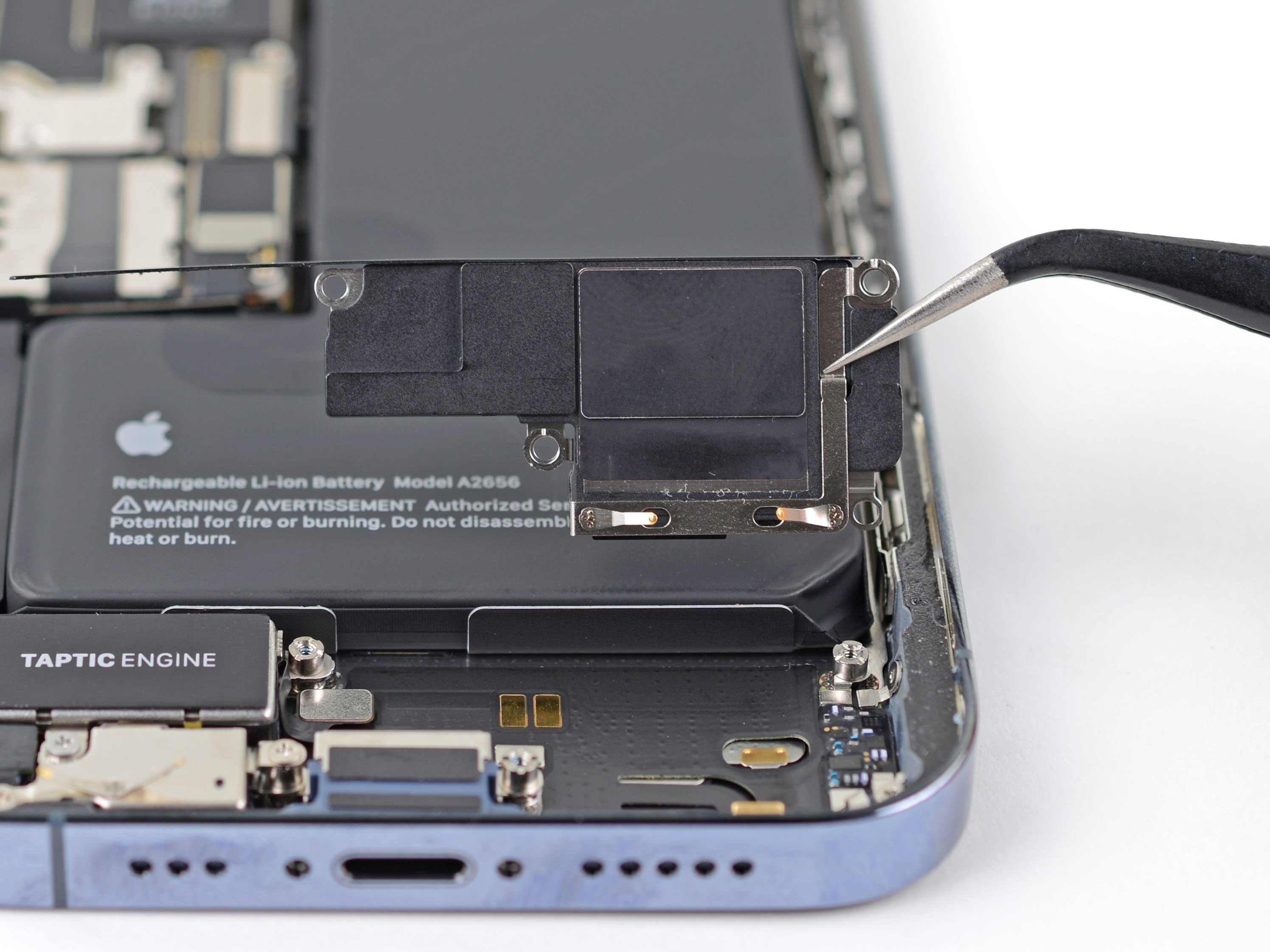
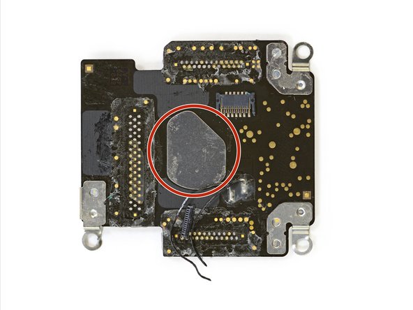
Just like everything in the Apple Watch, this battery was crafted to be sleek and ultra-thin. In contrast, larger gadgets like smartphones have bulkier batteries that soak up more X-rays, making them a breeze to detect.
- First thing you'll spot: the battery takes up a ton of real estate inside the watch, but it's practically a ghost in the X-ray—look for the hazy patch on the right.
- The real attention-grabbers in the X-ray are the magnets. They're the darkest bits you see—the speakers hanging out on the lower left, the Taptic Engine, and that little magnet in the center keeping the charger in line.
Step 3

- Comparing the Apple Watch to a Nike+ Sport GPS is like comparing apples to oranges—each has its own flavor!
- The Apple Watch is compact and packed tightly, leaving almost no room to spare. Plus, it boasts a visibly cool inductive charging coil.
- On the other hand, the Nike+ Sport GPS showcases larger screws, ample chip layouts, and sensors that extend beyond the main watch body.
Step 4


- Kick things off by tackling the Digital Crown—Apple made a big deal out of how cool this part is, so we’re giving it some attention. Inside, you'll find a tiny but classically designed mechanical component—think threaded bits and a solid bushing. As shown in our original teardown, the inside of the crown shaft has tiny notches, and just below that, an optical emitter or sensor reads these notches as they spin by. This setup acts as the encoder. If you need help, you can always schedule a repair.
Step 5

- As we move around the edge, you'll spot the side button catching your eye.
- Even through the X-ray, this button has that unmistakable Apple vibe.
- Sticking with the sleek style, Apple went with a design that’s pretty similar to the spring-loaded power button on the iPhone 6.
Step 6


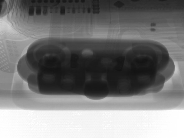
- The Taptic Engine, that little vibrating powerhouse, is one of the densest parts inside your watch — think of it as the core of the buzz. Thanks to some clever X-ray magic, we see that it’s basically a linear actuator, with springs that move a heavy weight up and down (and side to side on your wrist) to give you that satisfying tap. Apple packed this tiny, weighty component into the Taptic Engine to deliver maximum vibe in minimal space, giving your wrist a subtle but noticeable nudge. If you're curious about how vibration motors work in action, check out some cool videos of them running in real time inside X-ray machines. Need help? You can always schedule a repair.
Even though it’s a small component, it takes up quite a bit of the limited space inside the Apple Watch. Some folks might prefer that space for a bigger battery, but Apple clearly values the Taptic Engine as a key part of the overall experience. It’s a trade-off, and understanding that can help you appreciate why it’s tucked away where it is. If you need a hand with this, you can always schedule a repair.
Step 7

We’d love to get the inside scoop, but even X-rays can’t coax this Watch into sharing its secrets.
- Let’s turn our attention to the band-release button. It might look basic, but it’s actually packed with two layers of spring-loaded pins working together.
- Take a glance to the right of the band—there you'll spot the elusive diagnostic port, quietly waiting to be discovered.
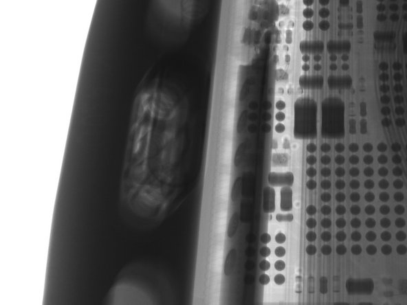
Step 8


The swirls and dots in the second image might look like tiny single-celled creatures, but nope—they're just some cool patterns. No biology lesson here, just some interesting visuals to keep in mind while you work.
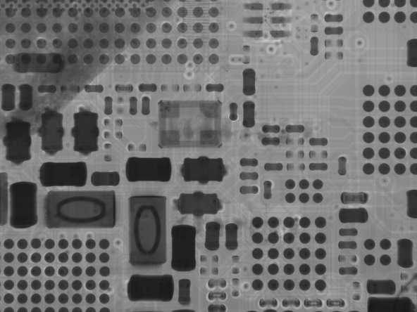
- Let's take a peek at what's hiding on the board: with a little X-ray magic, we can uncover the secrets of those tiny components.
- Check out the inductors - you can actually see the wire coils inside!
- Capacitors, on the other hand, are a bit more mysterious, with their wrapped dielectric layers keeping things under wraps.
- Resistors might be hard to spot, but look for the solder that's melted and formed a fillet on the edges - that's your clue.
- And then there are the invisible crystals, tucked away behind protective walls, but strategically placed near the processor to keep latency and signal interference at bay.
- Take a closer look and you'll see the wire coils of the inductive charger, the dark blobs that are solder mounts for a chip, and the wavy background pattern that's actually the flash memory chip - we'll dive deeper into that later...
Step 9

- The layout of the electronics is impressively precise. Chip-scale packages (CSPs) are scattered all over the board, and with such a snug fit, accuracy is essential—resulting in higher production costs.
- A big chunk of the expense comes from the board being densely packed with CSPs instead of the larger soldered packages.
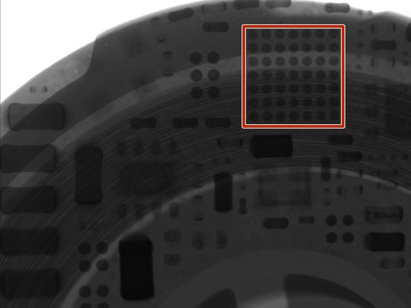
Step 10


- Check it out—the Apple S1 computer-on-chip in all its glory. Where things were a little hidden before, now we've got a solid view and some interesting details to share.
- Here's the one uncovered chip on the S1: an STMicroelectronics gyroscope and accelerometer, ready for action.
- Apple sealed the S1 in resin, which let them use wire bonding to connect chips in Package on Package (PoP) stacks. These wire bonds are seriously tiny, about 10-17 microns—think super-fine hair.
- This approach saves space (since soldered packages are chunkier), but pulling it off takes some real manufacturing wizardry.
Step 11


The A8 processor from the iPhone 6 (rocking a 20 nm process) actually outdoes the Apple Watch chip here, which takes a tiny step back in the tech timeline. And since the Apple Watch is basically glued to your wrist all day, power efficiency is even more of a big deal. With Samsung now rolling out chips at a super-tiny 14 nm, we're hoping the next Apple Watch will give your wrist more time between charges!
- Chipworks has been busy diving deep into the S1 over the past couple of weeks, and here’s the scoop:
- Take a peek at Chipworks' complete analysis right here.
- The Apple S1 System in Package (SiP) packs in over 30 components neatly arranged on a single board, which is then wrapped in a durable silica or aluminum composite resin—think of it like classic IC packaging, but for an entire board!
- At the core of the S1, we have Apple's snazzy APL0778 processor, crafted using Samsung's 28 nm LP process.
Step 12

- Check out the flash storage—it’s attached to the board with its solder points right on top. That pattern? Yeah, it threw us for a loop. Not your usual setup.
- Looking at the lines and vias on the chip, you’ll see this board is rocking four layers: two for signals, one for power, and one for ground. That’s some serious multitasking.
- Zoom in on the solder balls under the chip and you’ll spot some pale bubbles. That’s called voiding—don’t worry, it’s not a sci-fi villain.
- When you’re connecting boards, copper’s your go-to. But copper likes to rust faster than you can say 'oxidation.' Enter flux, the acid that helps solder stick. If there’s any flux left behind, you get voiding—those pesky bubbles.
- Too much voiding can be rough news for durability. Smooth, clean connections help heat escape, but if voiding takes over, heat gets trapped and your parts can overheat. Keep it clean for a longer-lasting device!
Step 13

Chances are, this is the heatsink chilling over the S1's super-compact processor. It's doing its best to keep things cool while the magic happens.
- Check out the weirdly-shaped metal blob at the center of the S1 - it's definitely worth a closer look. Under X-ray, it lines up neatly with the centering magnet for the charger, which makes us think Apple might have designed it to do double duty: aligning the charger and helping to dissipate heat from the S1 SiP.
- It's possible that this clever design choice is what helps keep your device running smoothly, so let's take a moment to appreciate the engineering that went into it.
Step 14


Hey, those little rectangles look pretty familiar, don’t they?
- Let's give that display a little sunshine and see if we’ve overlooked anything.
- It’s looking quite similar to what we spotted earlier—cables, chips, sensors, you name it!
- But wait, a closer look reveals what could be those nifty force touch strain gauges lurking at the bottom of the screen.
- The layout of the touchscreen controller and the ribbon cable paths seem like they were crafted by an artist rather than a tech wizard.
Step 15


As you can see, space is pretty limited in here, so let's work carefully!
- Capture some of the coolest shots with the X-ray bed — it’s adjustable and perfect for those sleek angled images that make it look like you're racing through a cityscape on the Grid. Check out the tiny screws embedded in the watch case; they’re like hidden gems. The delicate ribbon cable traces resemble tiny, colorful TRON metro maps — a blend of tech beauty and function. And remember, color shifts in the images reflect changes in density, just like greyscale images. If you need a hand with anything tricky, you can always schedule a repair.
Step 16
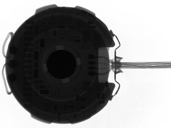


Tweak the power and exposure settings to reveal the different layers inside the charger—like magic, but with science!
- Lights down, spotlight up—let’s check out the inductive charger under the X-ray.
- X-ray tip: Power and current can be tweaked. If you want sharper images, dial down the power—just know that means fewer frames per second. Creative Electron’s machines can hit 60 FPS, but we took it slower for these shots.
- X-ray tip #2: The closer the tungsten sensor is to your part, the more zoomed-in you get. But, if the part is closer to the X-ray source, that zoom drops off.
- For example, in our first shot, you get a crisp outline of the charger’s guts, all wrapped in the fogginess of its plastic shell. By the last image, you’re seeing the tiny board components up close.
Step 17
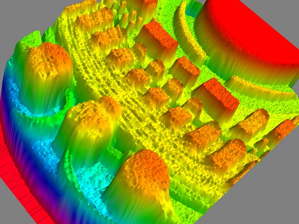


Check out this 3D graph! It shows how packed the inside of the charger is—taller spikes mean more stuff crammed in. That deep red half-circle? That’s the magnet. The bright yellow area marks the charging coils.
- Don't stress, this centering magnet is here to help, not harm - unless you're a tiny metal object, then it's got its eye on you. Either way, it ensures your device aligns perfectly for charging.
- Take a look at this clever charger. The inductive coils are at the bottom, and a weighty friend is at the top, keeping everything stable.
- Now, let's talk density. We've got a colorful map to guide you through this step.
Step 18

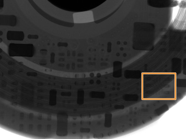
Every filament in the circuit links up different spots with its own resistor buddy.
- On the left, we have a lineup of dark coupling caps—likely working together in parallel. Those tiny, light-colored dots? Just some pesky little soldering voids left over from the manufacturing process.
- This charger is packing some serious brainpower! It likely knows the battery's charging profile, so the watch can just kick back and relax. Talk about saving space!
- The board may look a bit complex, but it’s actually just a single layer with no components on the bottom. Makes sense, right? It needs to lay flat for charging.
- Upon closer inspection, we discover a little resistor network hanging out.
- It's a one-layer PCB for power management—probably no thicker than 0.031 inches.
- At the top, we spot a sizable BGA (ball grid array), which likely indicates the presence of a power management IC.
Step 19
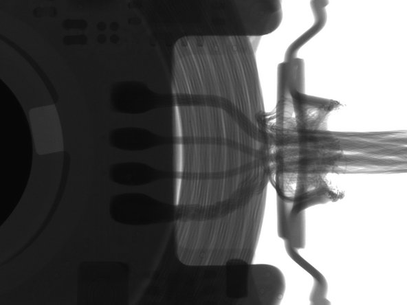
Attention savvy shoppers, this isn't your average charger!
- Guess what? X-rays have uncovered a little hidden gem: cable strain relief!
- This nifty springy piece of metal comes with some bonus wire coiled around it, ensuring that even if you give it a good tug, the cable stays snugly attached and doesn't go flying off into the void.
- Kudos to Apple for thinking ahead; this clever design might just outlast the very watch it's built to charge!
Step 20

- Big thanks to our partners who help us bring you the best repair guides!
- We're excited to collaborate with them to give you the inside scoop on the latest gadgets.
- If you missed our last teardown, check out our original Apple Watch teardown and get ready to dive in!