
iPad FCC Teardown
Duration: 45 minutes
Steps: 18 Steps
Get ready for our hands-on iPad teardown on April 3—when our pre-ordered devices land, we'll dive right in and show you all the details!
Update 4/3: We’ve got our hands on a production iPad, and now you get to enjoy some super crisp photos of its insides! FCC Photo Analysis: The FCC kindly gave us a sneak peek at the WiFi iPad’s guts before it hit the shelves. Sure, they tried to keep the cool stuff covered with grey boxes, but we managed to dig up the unfiltered files! The WiFi iPad goes by Apple model A1219, and the 3G version is A1337. Apple's request to keep this under wraps until August 17th? Well, the FCC had other plans. Heads up: This isn’t the typical Salvation Repair teardown. The photos here aren’t our usual high-def, and working with low-res files isn’t ideal, but we’re making it work! Expect a full-on teardown coming April 3, as soon as we get our pre-ordered iPads. Update: 3G iPad—We’ve discovered internal shots of the 3G iPad, which won’t be out for at least another month! Check out step 14 for those. Looking for the best bits? Keep an eye out for updates as we roll them out.
Step 1


- We're taking it step by step, so feel free to jump into the comments if you've got thoughts! Want the sharpest resolution? Just log in and you'll see larger versions of each photo.
- Quick heads-up: This might be a preproduction board, and Apple might have swapped some suppliers since they sent the FCC a sample. So, take the info with a pinch of salt until we get our hands on a production model tomorrow.
- Looks like Apple went all-in on the epoxy this time—these chips are locked down pretty tightly. We've never seen this much before, so you know they're serious about making this thing tough.
- 2x Toshiba Flash
- Apple A4
- Broadcom BCM5973
Step 2


- Let's take a look at the bottom of the logic board, both with and without the EMI shield. This part is key for making sure everything stays nice and cool while working.
- Great news! Apple didn't solder the battery down—just like the iPhone 3G and 3GS. So if you ever need to replace the battery, it's a lot easier than you might expect!
- This board seems to be made by AT&S. It’ll be interesting to see if their logo sticks around on the final production board, since Apple usually doesn’t include their manufacturer’s marks. A little sneak peek into the production process!
Step 3

- This cable is the superstar that transfers signals from the dock connector straight to the logic board. Pretty nifty, huh?
- Apple, never one to skimp on features, has cleverly attached the wifi and bluetooth boards to this very cable. Multi-tasking at its finest!
- Just like with some of its other devices, the home button is refreshingly simple. It has two contact points that connect with pads on the display assembly. When you press the button, voilà! The circuit comes to life.
- Interestingly, this RF/data cable doesn't have any GPS features. Guess Apple decided to keep it streamlined!
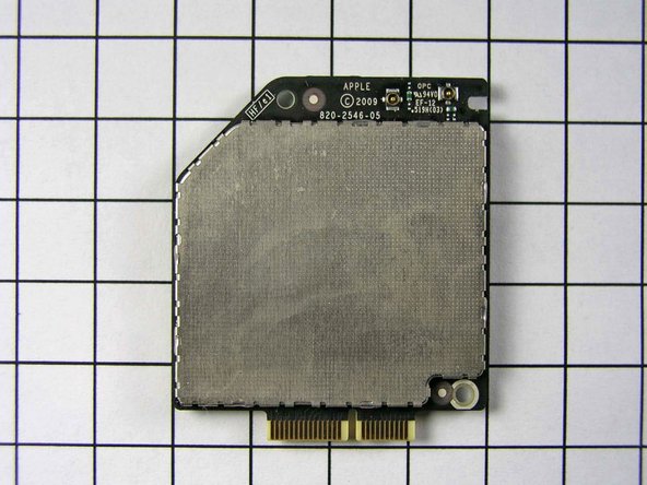
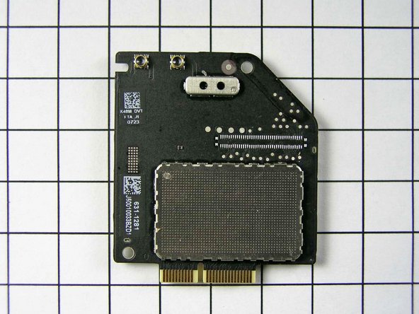
Step 4


- Wi-Fi and Bluetooth are buddies on the same board. Apple’s been hanging out with Broadcom lately, so chances are this is the trusty BCM4329 chip, just like in the 3rd Gen Touch.
- Check out the cover—laser engraving gives it that high-tech vibe:
- The bracket you see in picture two is multitasking: it keeps cables tidy and doubles as a ground point for the WiFi/Bluetooth/cable crew.
- X17B ES2.0-A4
- APN 339S0107
- USI 20091207
Step 5

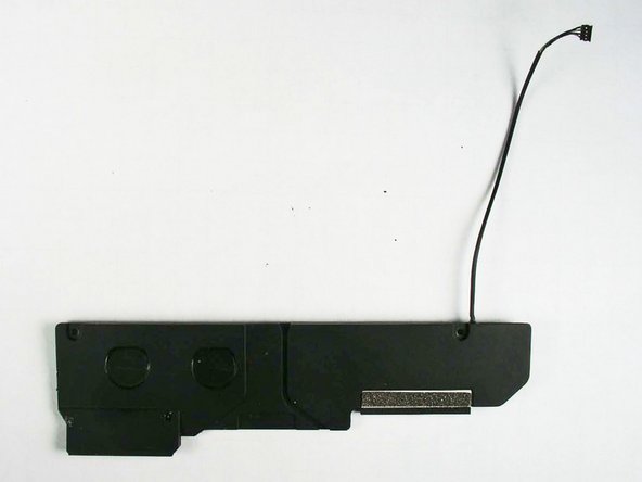
The connector on the speakers and other parts looks just like the ones in MacBook Unibody laptops. In other words, the iPad has a bit more breathing room inside than you might expect.
- A shot of the speaker assembly.
- The dual speakers deliver mono sound through two tiny sealed channels that funnel audio toward three ports cleverly carved into the bottom edge of the iPad.
Step 6


- Check out the inner side of the display assembly. It's where all the magic happens!
- The part number might be a bit tricky to read, but it seems to be LP097X02. If that's the case, this display is brought to you by LG-Phillips.
- Heads up! This is probably the priciest part of your iPad. It features top-notch IPS (in-plane switching) technology and is LED backlit, which is way cooler than the budget-friendly TN and CCFL options.
- Here are the display LED barcodes for your reference: 1579CN7346569 3225 LG0NJ 'GK65284221MTA', and 5091L-0942B 091214 R51 K319CED5D61R0094B2. Keep an eye out for them!
Step 7
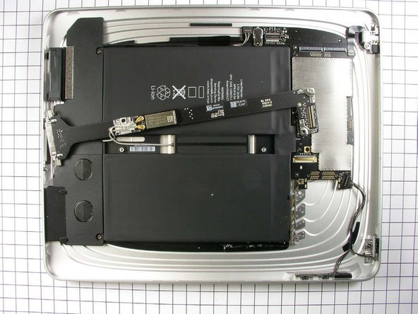
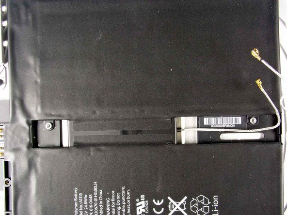

- Spotting the battery is a breeze in this shot of the rear case (minus the display assembly)—it’s the big, obvious component taking center stage.
- This powerhouse 3.75V, 24.8 watt-hour battery (that’s a hefty 6.5 amp hours!) keeps your device running for up to 10 hours, as advertised. For comparison: the iPhone 3GS rocks a 4.51 watt-hour battery, and the MacBook Air comes in at 40 watt-hours.
- It looks like the battery is made up of two separate 3.75V lithium polymer cells, wired together in parallel, so you get that epic battery life.
- The USB power supply for the iPad needed an upgrade to keep up! It’s a beefy 10W unit from Foxlink Technology, Ltd., with part # A1357 W010A051.
Step 8

- Check out some extra details on the battery:
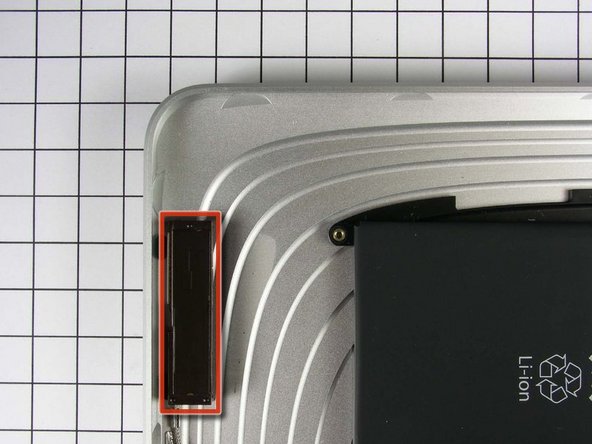
- That little black box you see in the second picture? That's one of the WiFi antennas, pretty nifty, right?
- Fingers crossed for solid WiFi reception! The back of the iPad is just a sleek block of aluminum. Besides the antenna we mentioned earlier, the Apple logo right in the middle of the rear case doubles as a window for RF signals to zip in and out. Apple has been pulling clever tricks like this for a while now, just like they did with the latest iMacs.
- APN: 616-0447
- VPN: DAK 120670-01HH00LH
Step 9

- Look at this solo iPad, chilling on its own!
- It’s probably hanging out inside a special RF interference testing lab, getting checked out by the FCC.
- This kind of test makes sure your device follows FCC Rules part 15 and Industry Canada RSS-210: basically, your iPad has to handle any interference that comes its way—even if it’s a bit annoying!
Step 10

- Check it out! Here's the iPad all hooked up to something called a LISN (Line Impedance Stabilization Network) – it's like the VIP lounge for EMI testing.
- And here we have the cool 10W USB power adapter, the stylish accessory from Apple that hit the shelves in late April.
Step 11

- Here’s the test setup used for the Specific Absorption Rate (SAR) report.
- The FCC is the host for this process.
- Check out the iPad manual for all the details.
- The SAR evaluation report for iPad (featuring 802.11abgn and Bluetooth Radios) is your go-to resource.
- There’s a ton of test data included in the FCC/IC Test Report, just in case you’re into that kind of thing.
Step 12

- The iPad model number A1219 is quite the conversation starter!
- A1219 is nestled right between the 1st Gen iPod Touch (A1213) and the MacBook Pro 15" Santa Rosa (A1226). Pretty neat, right?
- We might have imagined the iPad sporting a model number in the A13XX range instead of A12XX. It’s a bit of a puzzle, but our hunch is that it hints at a longer-than-usual development timeline.
- According to the FCC filing, the 3G version is labeled as model A1337. Is Apple just having a little fun with their model numbers? Who knows!
Step 13

- Here’s the bottom side of the iPad up close.
- Not a fan of those grainy, low-quality FCC photos? Wish your tax dollars went toward sharper, clearer shots of gadget internals? Stick around for tomorrow’s update when we break down the iPad with crisp 12.3 Megapixel images you’ll actually want to see.
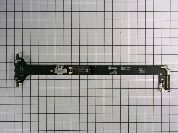
Step 14


- Check out this leaked FCC snapshot showing the communications board from the iPad 3G. It’s not linked on the main FCC page for the 3G model, so here it is for your reference.
- Parts:
- Infineon PMB 8878 X-Gold baseband IC.
- Skyworks SKY77340 Power Amplifier Module.
- Three Triquint power amplifier / filters.
- Infineon U6952.
- Numonyx 36MY1EE.
Step 15

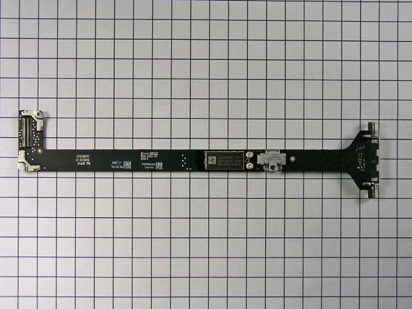
- Check out the Broadcom part hanging out on the top-left side—unfortunately, the FCC's photo is a bit too small to get a good look at it.
- Along the right side, you'll find three TriQuint power amplifiers: TQM616035A, TQM666032B, and TQM676031A. Fun fact: these are the very same trio of chips Apple packed into the iPhone 3G almost two years ago.
Step 16

- Check out this snap of the 3G communications board! It's looking good.
- Now, here's the scoop on the connector: it's got 25 pins in total, split into a crew of 15 and another group of 10.
- But hold on a sec! Just tossing this card into your iPad won't magically give you 3G. Nope! To get that snazzy 3G connectivity, you’ll need some extra antennas and a tweak to the rear casing.
Step 17

- Along the top edge of the iPad 3G's back case, you'll spot a black plastic strip—that’s where the signal magic happens. The big black plastic piece you see at the top of the photo? That’s the 3G antenna assembly doing its thing.
- See that quirky-looking part outlined in red? That’s the mounting spot for the 3G chip and maybe even the logic board. It’s welded right onto the rear case and probably acts as a grounding hub for the boards attached to it.
Step 18

- Check it out! The GPS antenna is hanging out on the back of the display assembly. It's that shiny gold foil piece you can spot near the top of the image.
- Now, for the display data cable connector—it's rocking the same style that we've seen in all the new Unibody MacBooks. Pretty neat, huh?


