Samsung Galaxy S III Teardown Guide: Step-by-Step Repair
Duration: 45 minutes
Steps: 13 Steps
Eager to get your hands on the Galaxy S 3? Let’s take a quick, fun look at the Samsung Galaxy S III, the worthy follow-up to the Galaxy S II. Thanks to Chipworks for the images! Stay connected for the latest updates on our teardowns!
Step 1

– Big shoutout to Chipworks for hooking us up with the awesome teardown pictures of the Galaxy S III. We appreciate their help in making this guide possible!
– Check out their full analysis on the Galaxy S III for all the nitty-gritty details.
Step 2


– The Samsung Galaxy S III, one of the most talked-about Android phones, comes packed with an impressive range of features. Here’s a rundown of the key specs that’ll make your tech-loving heart skip a beat:
– For a quick comparison, check out how it stacks up next to the Galaxy S2 (on the left).
– Operating System: Android 4.0 Ice Cream Sandwich
– Display: 4.8-inch Super AMOLED with a 720 x 1280 resolution – sharp and vibrant!
– Processor: 1.4 GHz quad-core powerhouse – speed is the name of the game.
– Battery: A solid 2100 mAh to keep you going throughout the day.
– Cameras: 8 MP rear-facing for those great photos and 1.9 MP front-facing for your selfie moments.
– Storage: Options for 16, 32, or 64 GB – plenty of space for all your apps, photos, and videos.
Step 3


– The sleek design of the latest Galaxy S features a straightforward power/sleep button tucked on the side of the device. As we prepare to get into this Galaxy S, it’s keeping an eye on us with its 8 MP rear camera. Flanking the camera are the flash and speaker assemblies. Not only is the Galaxy S watching us, but it’s also listening in. If you need help, you can always schedule a repair.
Step 4


Looks like Samsung wants us to check the manual before using the battery. Sure, that’s probably not happening, but hey, at least they asked!
– Just like in the Galaxy Nexus, the Samsung Galaxy S III sports a user-replaceable battery. The 3.8 V, 2100 mAh battery includes the antenna for the NFC (Near Field Communication) module used in ‘S Beam.’ If you’re curious, that 2100 mAh equals 7560 Coulombs of charge—roughly the same amount as what a 3.8V, 7.98 Wh battery can hold. Ready to get started? If you need a hand along the way, you can always schedule a repair.
Step 5


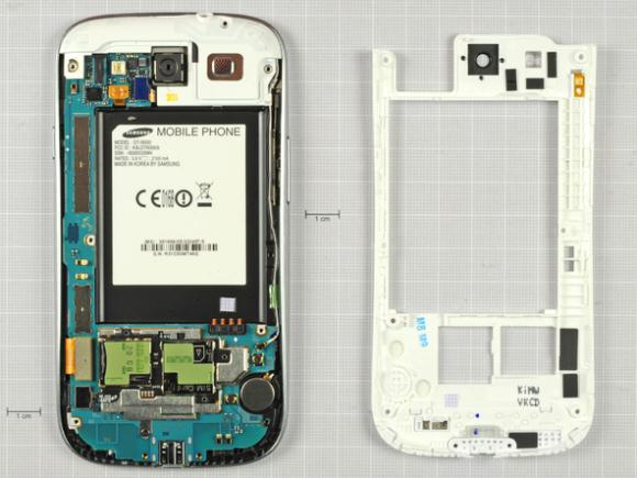
– Time to get inside! The spudger handles the first couple of plastic panels with ease.
– First up is the rear plastic frame—this piece shields the motherboard and hides a handy liquid indicator sticker.
– Removing this frame gives you straightforward access to the speaker assembly, which is simple enough to swap out.
Tools Used

Step 6


– Alright, time to figure out what to tackle first. So many parts packed into such a tiny space, it’s like a puzzle waiting to be solved!
– Rear-facing camera, huh? You bet! Let’s gently remove that 8 MP powerhouse from its cozy spot in the inner framework.
Step 7


– Next, carefully remove the motherboard from the inner support frame. Once the motherboard is out of the way, take a good look at the internal support structure. We think it might be magnesium, but we haven’t got the proof just yet. Lastly, spot a chip that’s not connected to the motherboard: it’s a Melfas 8PL533 Touch Sensor, responsible for translating your touch inputs into data. If you need help along the way, you can always schedule a repair.
Step 8
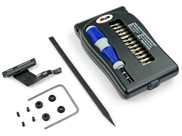

– Let’s chat about tools for a sec.
– We don’t just do repair guides—we offer parts and tools galore.
– Check out this sweet electronics tool kit we used to open up the new iPad. Trust us, it’ll earn its keep the first time you put it to work.
– Looking for Mac upgrades, iPhone screen repair parts, or even a kit to tackle the notorious Xbox Red Ring of Death? We’ve got you covered, and more.
– Your support helps us keep building the world’s best free repair resources.
Step 9

– Check out the front of the motherboard—looking sharp and packed with tech!
– Spot the Murata M2322007 WiFi Module ready to keep you connected.
– Here’s the heart of the device: a Samsung Exynos 4412 quad-core A9 processor with 1 GB LP DDR2 Green Memory (K3PE7E700M-XGC2).
– Samsung KMVTU000LM eMMC (16GB) + MDDR (64MB) NAND Flash is on board, handling all your storage needs.
– Say hello to the Intel Wireless PMB9811X Gold Baseband processor.
– You’ll also find the MAX77693 and MAX77686 chips doing their behind-the-scenes magic.
– Check out the Broadcom BCM47511 Integrated Monolithic GNSS Receiver for all your navigation power.
– 33ODC 2214 4TP AC—just another piece to the motherboard puzzle.
Step 10

– Let’s take a look at the bottom of the motherboard. Here, you’ll find some important components keeping everything running smoothly.
– First up, we have the Wolfson Microelectronics WM1811 stereo codec, which handles all your audio magic.
– Next, there’s the Skyworks SKY77604 Multi-Band Power amplifier, boosting your signal to keep you connected.
– The Silicon Image 9244 low-power MHL Transmitter is in charge of streaming video and audio with minimal energy use—pretty cool, right?
– Then we have the NXP PN544 NFC Chip, making sure all your near-field communication tasks happen seamlessly.
– Last but not least, the Infineon PMB5712 RF transceiver is here, helping with your radio frequency communication needs.
Step 11

– The glass is stuck to the display, and the display is attached to the frame of the Galaxy S III. It’s like a tight-knit family—everyone’s connected!
– This setup can make replacing the glass a bit more expensive if you happen to break it. So, it’s definitely something to keep in mind while handling your device!
Step 12

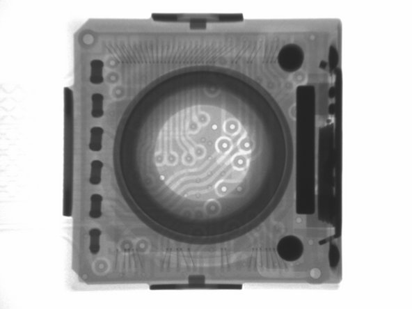
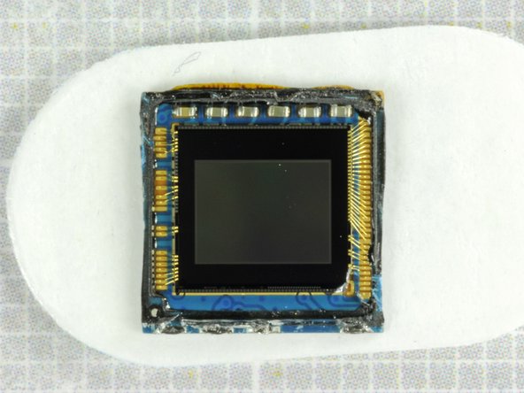
– Let’s take a closer look at that intriguing camera with some detailed shots, including a Chipworks x-ray! According to Chipworks, the sensor inside is a Sony BSI sensor. Interestingly, their initial inspection suggests it’s a brand-new sensor, not the same one found in the iPhone 4S. The bond pad layout doesn’t match the IMX145 used in the iPhone 4S, nor does it resemble the IMX105 seen in earlier Samsung models. Keep this in mind as you work through the repair, and if you need a hand, you can always schedule a repair.
Step 13


– Update: We first checked out the Galaxy SIII teardown from afar, but now that we’ve had our hands on it, we’re ready to drop a real repairability score:
– Samsung Galaxy SIII Repairability Score: 8 out of 10 (with 10 being a breeze).
– The battery pops out without any tools—nice and simple.
– Popping the phone open and getting to the guts is a walk in the park.
– Just 12 screws in the whole device, all standard Phillips #0—no weird sizes or secret tools needed.
– Small parts like antennas, the vibrator, and the light sensor are easy to swap since they’re modular, though they’re stuck to the front panel.
– The not-so-great news: the glass is glued to both the display and the frame, so swapping that out isn’t cheap.
– To get to the front panel, you’ll have to disassemble the whole phone, since all the good stuff lives in the back.
Success!